What happened
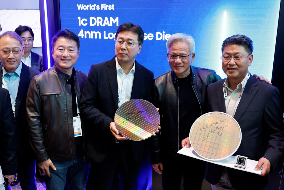
Reuters cited Seoul Economic Daily reporting that Samsung will use TSMC's 3nm process for base dies in Nvidia's custom high-bandwidth memory.
The report says Nvidia requested the same base-die process from Samsung, SK Hynix, and Micron.
Samsung reportedly plans to retain its own manufacturing approach for standard HBM and other customers.
Why it matters
AI accelerator performance depends increasingly on memory bandwidth, controllers, and advanced packaging.
Custom memory designs can require cooperation between competing semiconductor manufacturers.
Key numbers & facts
- 3-nanometre process reported for NVHBM base dies.
- Three memory suppliers named: Samsung, SK Hynix, and Micron.
- Nvidia's NVHBM design integrates a custom controller into the base die.
Practical implications
- Benchmark memory bandwidth, capacity, and data movement alongside compute throughput.
- Optimize inference serving for the actual accelerator memory hierarchy.
- Track foundry and packaging concentration in hardware procurement.
Likely future impact
Analysis, not a confirmed outcome.
- Custom HBM could increase chipmakers' reliance on specialized foundry processes.
- Memory-aware AI software optimizations may grow in importance.
Evidence
- Source: https://www.reuters.com/world/asia-pacific/samsung-use-tsmc-technology-nvidias-next-generation-memory-chips-seoul-newspaper-2026-10-18/
What remains uncertain
- The reported arrangement was not independently confirmed by all parties.
- Production volume, yield, pricing, and shipment timing are unconfirmed.